Mitigating Thin-Glass Warpage in the Deposition Process
As device architectures continue to adopt thinner and lighter glass substrates, manufacturers face increasing challenges during vacuum deposition and related thin-film processes. One persistent issue is the warpage of thin glass, which can prevent substrates from advancing through subsequent process steps and ultimately reduce throughput and yield.
This case study highlights how applying a carrier glass to reinforce thin substrates offers an effective and practical solution to suppress warpage and maintain stable line operation throughout the deposition process.
01/Background: Warpage Challenges in Thin-Glass Deposition
 In thin-film device manufacturing—including sensors, display components, and advanced packaging—deposition onto thin glass substrates (e.g., around 0.5 mm thickness) is increasingly common.
However, these ultra-thin substrates are highly susceptible to mechanical deformation during film growth.
Typical problems include:
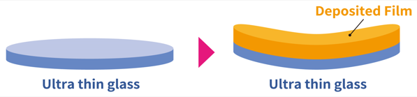
・Process-induced warpage: Stress from deposited layers—especially metal layers such as thick copper—can cause the glass to bow significantly.
・Transport failures: Warped wafers may not align with handling systems, causing stoppages or requiring manual intervention.
・Yield loss: Non-uniform deposition due to bending leads to variations in film thickness and degraded device performance.
・Process limitations: Certain high-stress films cannot be applied to thin substrates without the risk of severe deformation.
In many cases, depending on the deposited films, warpage becomes a significant concern when the glass thickness falls below 0.5 mm, making thin-glass processing difficult without additional reinforcement.
02/AGC’s Solution: Carrier-Glass Lamination to Suppress Warpage
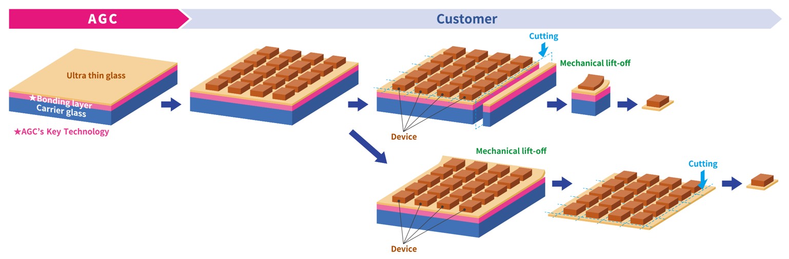
To overcome these issues, AGC proposes a carrier-glass lamination method that mechanically reinforces the thin substrate before it enters the deposition process.
By bonding a carrier glass to the thin glass, the overall composite thickness increases, dramatically improving rigidity and suppressing stress-induced deformation.
Key Advantages:
・Effective warpage suppression: Increased composite stiffness prevents bending caused by high-stress film deposition such as thick Cu layers.
・Stable process flow: Improved flatness allows the substrate to move smoothly through deposition chambers and downstream processes.
・High compatibility: The method adapts easily to a variety of deposition conditions and film types, supported by a bonding layer with excellent heat resistance and chemical durability.
・Scalability and practicality: Carrier lamination can be integrated into existing workflows with minimal modification.
・Yield improvement: Ensures uniform film formation across the entire substrate.
By reinforcing the thin glass with a dedicated carrier, manufacturers can maintain high-quality deposition results, minimize downtime, and unlock process capabilities that would otherwise be difficult to achieve with thin glass alone.
03/Explore AGC’s Advanced Glass Technologies
AGC continues to pioneer advanced glass technologies that enable safer, more reliable, and higher‐yield manufacturing for next‐generation electronic devices.
To learn more about AGC’s carrier glass technology for thin glass handling, please visit the official product page.